Modbus Guide
This guide explains how Modbus RTU and Modbus TCP work, how to read frames and registers, how to convert raw register values, and how to troubleshoot common communication problems.
Overview
Modbus is a simple, royalty-free application-layer protocol. The client sends a request and the server responds—the server does not send messages on its own initiative. Terminology has been updated from master/slave → client/server.
1.1 Hexadecimal
Modbus messages travel as bits (0/1). Four bits form an easy-to-read hexadecimal digit (0–F), so binary data is almost always presented in hex. The hexadecimal system has a base of 16. In practice, Modbus messages are commonly converted from binary form to hexadecimal to make them easier to read. You’ll need to interpret hex during commissioning and troubleshooting.
A bit is the smallest unit of information (0 or 1).
- One hex digit represents four bits.
- Byte = 8 bits = two hex digits.
- 16‑bit register = 2 bytes = four hex digits.
Bit string 0001 0010 1011 1100 in hexadecimal is 0x12BC.
| N1 | N2 | N3 | N4 | |
|---|---|---|---|---|
| BIN | 0001 | 0010 | 1011 | 1100 |
| HEX | 1 | 2 | B | C |
The table below shows how each 4-bit binary value maps to one hexadecimal digit.
| 0000 = 0 | 0100 = 4 | 1000 = 8 | 1100 = C |
| 0001 = 1 | 0101 = 5 | 1001 = 9 | 1101 = D |
| 0010 = 2 | 0110 = 6 | 1010 = A | 1110 = E |
| 0011 = 3 | 0111 = 7 | 1011 = B | 1111 = F |
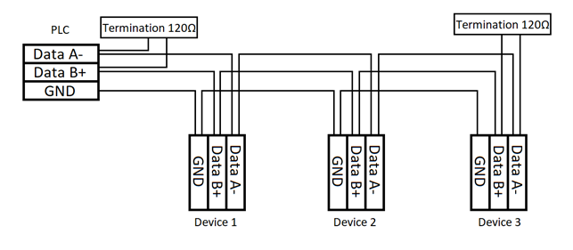
1.2 Modbus RTU bus wiring and voltage levels
The Modbus RTU message is transmitted through a serial bus. Branches in the bus should be avoided, as they cause communication problems. The bus is usually terminated at both ends with a 120Ω resistor. The purpose of this resistor is to prevent reflections and thus reduce interference in bus communication.
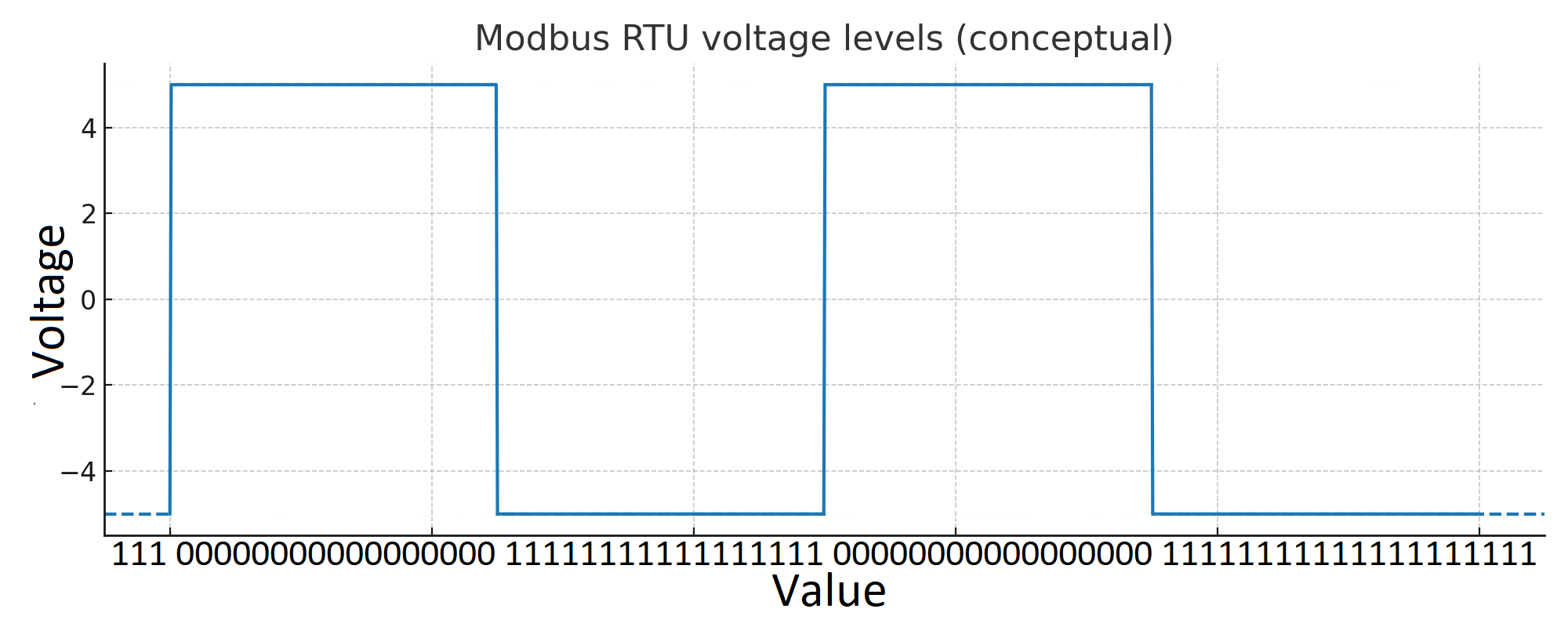
In Modbus RTU messages (RS-485), the bus voltage level varies between +5 and -5 volts. A voltage of -5V corresponds to a bit value of 1, and a voltage of +5V corresponds to a bit value of 0. A voltage of 0V means that there is a pause in communication.
1.3 Modbus RTU bus cable
For RS-485 buses, a twisted pair cable with as much shielding as possible should be used. The better the shielding, the fewer disturbances occur in the bus.
RS-485 communication is based on differential signal transmission, where the cable conductors form a twisted pair. This structure effectively reduces electromagnetic interference from external sources such as frequency converters, relays, and other devices using high currents. In addition, the shielding helps to prevent interference from coupling into the bus and also reduces emissions from the bus into the environment.
Special attention should be paid to grounding and connecting the cable shield. It is generally recommended that the shield is grounded only at one end to avoid ground loops caused by potential differences.
1.4 Modbus RTU bus speed and maximum length
The performance of the Modbus RTU bus is significantly affected by the transmission speed (baud rate) and the cable length used. The higher the speed, the shorter the maximum bus length:
- 9600 bps → up to about 1200 m
- 19200 bps → about 600 m
- 38400 bps → about 300 m
- 115200 bps → about 100 m
The values above are guidelines, and the actual maximum lengths depend on the cable type, installation conditions, and interference environment. In noisy environments, it is recommended to use a lower speed and ensure good cable quality and grounding.
1.5 Reflections in the cable
When a reflection occurs, the electrical signal “bounces back” and distorts the bus voltage levels. Distorted voltage levels lead to communication errors.
To prevent reflections as effectively as possible, the termination resistor should match the characteristic impedance of the cable used. For example, in Finland the commonly used Nomak cable has a characteristic impedance of 75Ω, in which case the termination resistors should also be 75Ω. If a 75Ω cable is used with 120Ω termination resistors, reflections occur with a coefficient of |Γ| ≈ 0.23. In practice, such a bus is usually functional despite the impedance mismatch.
1.6 Principle of termination
The purpose of the termination resistor is to absorb the signal at the end of the cable so that it does not reflect back into the line. If the bus is long and the speed is high, without termination the signals are easily distorted and the messages become difficult to read. Termination resistors are always placed at both ends of the bus.
1.7 Biasing and idle state
Termination alone is not enough if the bus remains floating in an idle state. In such a case, the receiver inputs may remain undefined and generate erroneous bit interpretations. For this purpose, biasing resistors are used, which set a small DC voltage difference between the A and B lines of the bus. Typically, biasing is implemented with a single resistor pair at one point in the bus, most often at the master device.
1.8 Practical considerations
- Only one pair of termination resistors: Termination should only be done at the two ends of the bus. If there are more terminations, the signal is attenuated too much and communication may be disrupted.
- Cable length and speed: The longer the bus and the higher the baud rate, the more critical correct termination becomes. On short cables and at low speeds, the bus can often operate without termination.
- Impedance mismatch: In practice, buses often work quite reliably even with some impedance mismatch, but the closer the termination matches the cable’s characteristic impedance, the fewer errors occur.
1.9 Client and server
There are two device roles in Modbus: Client (Master) and Server (Slave). In a Modbus RTU network there is typically one client and up to 255 servers. Each server is assigned a unique Modbus address from 1–255. Avoid using address 1, as it is a common default and easily causes conflicts in practice.
- The client reads or writes registers. Usually a PLC.
- The server returns values or stores them on request. Usually a field device.
- The server does not send messages without a request.
1.10 Registers
There are four types of Modbus registers (Coil, Discrete Input, Input Register, Holding Register). They differ in size (1 bit / 16 bits) and access rights (R/W). Vendor documentation may use either the 1…49999 or the 0…65535 register space. Registers may also have vendor‑specific restrictions that deviate from the standard, such as write limitations on Coil registers or a limit on how many registers can be read at once.
| Register type | Access | Size | Address |
|---|---|---|---|
| Coil | Read/write | 1-bit | 1–9999 (0–65535) |
| Discrete input | Read only | 1-bit | 10001–19999 (0–65535) |
| Input register | Read only | 16-bit | 30001–39999 (0–65535) |
| Holding register | Read/write | 16-bit | 40001–49999 (0–65535) |
Also note 0- vs 1-based indexing for the starting register—always check the device datasheet.
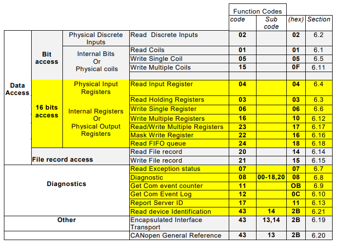
1.11 Function codes
Function codes are one‑byte commands used to read/write a given register type at one or more addresses. In addition to the standard codes, some devices may have manufacturer‑specific codes, and not all devices necessarily support every code. Below is a quick view of the official function codes from modbus.org.
1.12 CRC (Cyclic Redundancy Check)
Each RTU frame ends with a 16‑bit CRC. The sender and receiver compute the CRC from the message bytes and compare the results; a change in even a single bit causes an error.
1.13 Parity
Parity can be N (none), E (even), or O (odd). The parity setting must match on both ends, otherwise errors occur. The parity bit ensures the number of bits with value 1 in the frame has the defined even/odd parity. If there would be an odd number of 1s and parity is set to E, the parity bit switches to one (1).
1.14 Byte and word order (endianness)
Modbus register values are transferred as bytes. For single 16-bit registers this is usually straightforward, but 32-bit and 64-bit values are built from multiple registers, and devices may use different byte or word orders.
By default, Modbus register data is commonly shown in big-endian order, where the most significant byte is listed first. However, some devices swap the two 16-bit words of a 32-bit value, swap bytes inside each word, or do both.
For this reason, the byte order and word order must always be checked from the device-specific register map.
Common 32-bit orders include:
| Order | Meaning |
|---|---|
ABCD | normal big-endian order |
CDAB | word swapped |
BADC | bytes swapped inside each word |
DCBA | bytes and words swapped / little-endian order |
A practical example is shown in section 1.16 Converting raw register values.
1.15 Data types
In Modbus, internal device variables such as temperatures, states, alarms, counters, and setpoints are transferred as registers and bit values. The Modbus protocol itself does not define whether a register contains a signed integer, unsigned integer, floating-point value, status word, or scaled engineering value.
A Modbus register is 16 bits. This means one register can directly contain a 16-bit value, while larger values are formed by combining multiple consecutive 16-bit registers.
1 register  = 16 bits
2 registers = 32 bits
4 registers = 64 bits
Common Modbus data types include:
| Data type | Size | Register count |
|---|---|---|
BOOL / bit | 1 bit | coil or discrete input |
UINT16 | 16 bits | 1 register |
INT16 | 16 bits | 1 register |
UINT32 | 32 bits | 2 registers |
INT32 | 32 bits | 2 registers |
FLOAT32 | 32 bits | 2 registers |
UINT64 | 64 bits | 4 registers |
INT64 | 64 bits | 4 registers |
FLOAT64 / DOUBLE | 64 bits | 4 registers |
The client must know the correct data type from the device documentation. If the wrong data type is selected, the device may respond correctly, but the displayed value will be wrong.
For example, the same raw 16-bit register can be interpreted as UINT16 or INT16. The same two consecutive registers can be interpreted as UINT32, INT32, or FLOAT32. For 32-bit and 64-bit values, the byte order and word order also matter.
Practical examples of signed and unsigned values, byte order, word order, scaling, offsets, and wrong-value troubleshooting are shown in section 1.16 Converting raw register values.
1.16 Converting raw register values
When reading Modbus registers, communication can work correctly even if the displayed value is wrong. This usually means that the device responds to the request, but the client interprets the returned register data with the wrong data type, byte order, word order, scaling factor, offset, or register address.
A valid Modbus response does not automatically mean that the engineering value is correct.
One register is 16 bits
A Modbus register contains 16 bits:
1 register = 16 bits = 2 bytes = 4 hex digits
One register can directly hold 16-bit values:
| Data type | Size | Register count |
|---|---|---|
UINT16 | 16 bits | 1 register |
INT16 | 16 bits | 1 register |
Larger values are formed from multiple consecutive registers:
| Data type | Size | Register count |
|---|---|---|
UINT32 | 32 bits | 2 registers |
INT32 | 32 bits | 2 registers |
FLOAT32 | 32 bits | 2 registers |
UINT64 | 64 bits | 4 registers |
INT64 | 64 bits | 4 registers |
FLOAT64 / DOUBLE | 64 bits | 4 registers |
If the device documentation says that a value is FLOAT32, the client must read two consecutive registers and combine them correctly.
Signed and unsigned values
The same raw 16-bit register can produce different values depending on whether it is interpreted as signed or unsigned.
Example:
Raw register = 0xFF9C
| Data type | Value |
|---|---|
UINT16 | 65436 |
INT16 | -100 |
As an unsigned value, 0xFF9C means 65436. As a signed 16-bit value, using two’s complement, it means -100.
This matters for values that may go below zero, such as outdoor temperature, pressure difference, offsets, control corrections, and power import/export values.
If the scale factor is 0.1, the final value is:
-100 x 0.1 = -10.0 °C
32-bit values from two registers
A 32-bit value is built from two 16-bit registers.
Example:
Register 1 = 0x42F6
Register 2 = 0x0000
The raw bytes are:
42 F6 00 00
The same bytes can be interpreted in different ways:
| Data type | Example result |
|---|---|
UINT32 | 1123418112 |
INT32 | 1123418112 |
FLOAT32 | 123.0 |
The raw data is identical. Only the interpretation changes.
Byte and word order
A 32-bit value consists of four bytes, often described as:
A B C D
Because Modbus registers are 16-bit, the value is split into two registers:
Register 1 = A B
Register 2 = C D
Common 32-bit byte and word orders are:
| Order | Description | Byte sequence |
|---|---|---|
ABCD | Normal big-endian order | A B C D |
CDAB | Word swapped | C D A B |
BADC | Byte swapped inside each word | B A D C |
DCBA | Byte and word swapped | D C B A |
Using the example registers:
Register 1 = 0x42F6
Register 2 = 0x0000
The possible byte sequences are:
| Order | Byte sequence | FLOAT32 result |
|---|---|---|
ABCD | 42 F6 00 00 | 123.0 |
CDAB | 00 00 42 F6 | very small value |
BADC | F6 42 00 00 | unrealistic value |
DCBA | 00 00 F6 42 | very small value |
This is one of the most common reasons why a Modbus value looks wrong even though the request and response are valid.
Scaling and offset
Many devices send an integer value that must be converted into an engineering value.
Engineering value = raw value x scale factor
Example:
Raw value = 234
Scale factor = 0.1
Engineering value = 234 x 0.1 = 23.4 °C
Some devices also use an offset:
Engineering value = raw value x scale factor + offset
Example:
Raw value = 234
Scale factor = 0.1
Offset = -50
Engineering value = 234 x 0.1 - 50 = -26.6
The scale factor, offset, and unit must be checked from the device-specific register map.
Address, register type, and function code
Wrong values can also come from reading the wrong place.
Some manuals document holding registers as 40001, 40002, 40003, while the actual Modbus request uses zero-based addresses 0, 1, 2. This means that a register documented as 40001 may need to be requested as address 0.
Also check that the correct register area and function code are used:
| Register type | Typical function code | Access | Size |
|---|---|---|---|
| Coil | 01 / 05 / 15 | read/write | 1 bit |
| Discrete Input | 02 | read only | 1 bit |
| Input Register | 04 | read only | 16 bits |
| Holding Register | 03 / 06 / 16 | read/write | 16 bits |
Reading address 10 with Function Code 03 is not the same as reading address 10 with Function Code 04.
Troubleshooting method
Start with the raw register values before converting them into engineering units.
For one-register values, compare:
| Raw register | UINT16 | INT16 |
|---|---|---|
0xFF9C | 65436 | -100 |
For two-register values, compare:
| Interpretation | What it checks |
|---|---|
UINT32 ABCD | normal unsigned 32-bit value |
INT32 ABCD | normal signed 32-bit value |
FLOAT32 ABCD | normal floating-point value |
FLOAT32 CDAB | word-swapped floating-point value |
FLOAT32 BADC | byte-swapped floating-point value |
FLOAT32 DCBA | byte- and word-swapped floating-point value |
If one interpretation produces a realistic value and the others produce unrealistic values, the realistic one is usually the intended format.
Common reasons for wrong Modbus values
- wrong register address
- 0-based vs 1-based address confusion
- wrong register type or function code
- signed value interpreted as unsigned, or the opposite
- 32-bit value read as 16-bit
- wrong byte order or word order
- missing scale factor or offset
- wrong unit
- copied conversion settings from another register
Always check the device-specific register map and record the raw register values when troubleshooting.
1.17 Example messages
Read Coils: Function Code 01
Request: 01 01 00 05 00 03 6C 0A
| Bytes | Field | Value |
|---|---|---|
| 01 | Modbus address | 0x01 (1) |
| 01 | Function code | 0x01 (1) — Read Coils |
| 00 05 | Starting address | Base‑0: 0x0005 (5) · Base‑1: 0x0006 (6) |
| 00 03 | Quantity | 0x0003 (3) |
| 6C 0A | CRC | 0x6C0A (27658) |
Response: 01 01 01 02 D0 49
| Bytes | Field | Value |
|---|---|---|
| 01 | Modbus address | 0x01 (1) |
| 01 | Function code | 0x01 (1) — Read Coils |
| 01 | Byte count | 0x01 (1) |
| 02 | Data for coils 5, 6 and 7 | 0x02 |
| Bits (bN=Value, LSB→MSB per byte) | b0=0, b1=1, b2=0, b3=0, b4=0, b5=0, b6=0, b7=0 | |
| D0 49 | CRC | 0xD049 (53321) |
Read Discrete Inputs: Function Code 02
Request: 01 02 00 02 00 02 58 0B
| Bytes | Field | Value |
|---|---|---|
| 01 | Modbus address | 0x01 (1) |
| 02 | Function code | 0x02 (2) — Read Discrete Inputs |
| 00 02 | Starting address | Base‑0: 0x0002 (2) · Base‑1: 0x0003 (3) |
| 00 02 | Quantity | 0x0002 (2) |
| 58 0B | CRC | 0x580B (22539) |
Response: 01 02 01 00 A1 88
| Bytes | Field | Value |
|---|---|---|
| 01 | Modbus address | 0x01 (1) |
| 02 | Function code | 0x02 (2) — Read Discrete Inputs |
| 01 | Byte count | 0x01 (1) |
| 00 | Data for inputs 2 and 3 | 0x00 |
| Bits (bN=Value, LSB→MSB per byte) | b0=0, b1=0, b2=0, b3=0, b4=0, b5=0, b6=0, b7=0 | |
| A1 88 | CRC | 0xA188 (41352) |
Read Holding Registers: Function Code 03
Request: 01 03 00 07 00 02 75 CA
| Bytes | Field | Value |
|---|---|---|
| 01 | Modbus address | 0x01 (1) |
| 03 | Function code | 0x03 (3) — Read Holding Registers |
| 00 07 | Starting address | Base‑0: 0x0007 (7) · Base‑1: 0x0008 (8) |
| 00 02 | Quantity | 0x0002 (2) |
| 75 CA | CRC | 0x75CA (30154) |
Response: 01 03 04 00 01 00 06 2B F1
| Bytes | Field | Value |
|---|---|---|
| 01 | Modbus address | 0x01 (1) |
| 03 | Function code | 0x03 (3) — Read Holding Registers |
| 04 | Byte count | 0x04 (4) |
| 00 01 00 06 | Data for registers 7 and 8 | 0x0001 (1), 0x0006 (6) |
| 2B F1 | CRC | 0x2BF1 (11249) |
Read Input Registers: Function Code 04
Request: 01 04 00 00 00 02 71 CB
| Bytes | Field | Value |
|---|---|---|
| 01 | Modbus address | 0x01 (1) |
| 04 | Function code | 0x04 (4) — Read Input Registers |
| 00 00 | Starting address | Base‑0: 0x0000 (0) · Base‑1: 0x0001 (1) |
| 00 02 | Quantity | 0x0002 (2) |
| 71 CB | CRC | 0x71CB (29131) |
Response: 01 04 04 00 01 00 0B EB 83
| Bytes | Field | Value |
|---|---|---|
| 01 | Modbus address | 0x01 (1) |
| 04 | Function code | 0x04 (4) — Read Input Registers |
| 04 | Byte count | 0x04 (4) |
| 00 01 00 0B | Data for registers 0 and 1 | 0x0001 (1), 0x000B (11) |
| EB 83 | CRC | 0xEB83 (60291) |
Write Single Coil: Function Code 05
Request: 16 05 00 09 00 00 1E EF
| Bytes | Field | Value |
|---|---|---|
| 16 | Modbus address | 0x16 (22) |
| 05 | Function code | 0x05 (5) — Write Single Coil |
| 00 09 | Coil address | Base‑0: 0x0009 (9) · Base‑1: 0x000A (10) |
| 00 00 | Data for coil 9 | B1:1 |
| 1E EF | CRC | 0x1EEF (7919) |
Response: 16 05 00 09 FF 00 5F 1F
| Bytes | Field | Value |
|---|---|---|
| 16 | Modbus address | 0x16 (22) |
| 05 | Function code | 0x05 (5) — Write Single Coil |
| 00 09 | Coil address | Base‑0: 0x0009 (9) · Base‑1: 0x000A (10) |
| FF 00 | Data for coil 9 | B0:1 |
| 5F 1F | CRC | 0x5F1F (24351) |
Write Single Register: Function Code 06
Request: 16 06 00 09 00 01 9B 2F
| Bytes | Field | Value |
|---|---|---|
| 16 | Modbus address | 0x16 (22) |
| 06 | Function code | 0x06 (6) — Write Single Register |
| 00 09 | Register address | Base‑0: 0x0009 (9) · Base‑1: 0x000A (10) |
| 00 01 | Data for register 9 | 0x0001 (1) |
| 9B 2F | CRC | 0x9B2F (39727) |
Response: 16 06 00 09 00 01 9B 2F
| Bytes | Field | Value |
|---|---|---|
| 16 | Modbus address | 0x16 (22) |
| 06 | Function code | 0x06 (6) — Write Single Register |
| 00 09 | Register address | Base‑0: 0x0009 (9) · Base‑1: 0x000A (10) |
| 00 01 | Data for register 9 | 0x0001 (1) |
| 9B 2F | CRC | 0x9B2F (39727) |
Write Multiple Coils: Function Code 15
Request: 16 0F 00 09 00 05 01 0D 32 78
| Bytes | Field | Value |
|---|---|---|
| 16 | Modbus address | 0x16 (22) |
| 0F | Function code | 0x0F (15) — Write Multiple Coils |
| 00 09 | Starting address | Base‑0: 0x0009 (9) · Base‑1: 0x000A (10) |
| 00 05 | Quantity | 0x0005 (5) |
| 01 | Byte count | 0x01 (1) |
| 0D | Data for coils 9–13 | 0x0D |
| Bits (bN=Value, LSB→MSB per byte) | b0=1, b1=0, b2=1, b3=1, b4=0, b5=0 | |
| 32 78 | CRC | 0x3278 (12920) |
Response: 16 0F 00 09 00 05 46 ED
| Bytes | Field | Value |
|---|---|---|
| 16 | Modbus address | 0x16 (22) |
| 0F | Function code | 0x0F (15) — Write Multiple Coils |
| 00 09 | Starting address | Base‑0: 0x0009 (9) · Base‑1: 0x000A (10) |
| 00 05 | Quantity | 0x0005 (5) |
| 46 ED | CRC | 0x46ED (18157) |
Write Multiple Registers: Function Code 16
Request: 16 10 00 09 00 05 0A 00 09 00 02 00 4D 00 00 00 01 13 5B
| Bytes | Field | Value |
|---|---|---|
| 16 | Modbus address | 0x16 (22) |
| 10 | Function code | 0x10 (16) — Write Multiple Registers |
| 00 09 | Starting address | Base‑0: 0x0009 (9) · Base‑1: 0x000A (10) |
| 00 05 | Quantity | 0x0005 (5) |
| 0A | Byte count | 0x0A (10) |
| 00 09 00 02 00 4D 00 00 00 01 | Data for registers 9–13 | 0x0009 (9), 0x0002 (2), 0x004D (77), 0x0000 (0), 0x0001 (1) |
| 13 5B | CRC | 0x135B (4955) |
Response: 16 10 00 09 00 05 D3 2F
| Bytes | Field | Value |
|---|---|---|
| 16 | Modbus address | 0x16 (22) |
| 10 | Function code | 0x10 (16) — Write Multiple Registers |
| 00 09 | Starting address | Base‑0: 0x0009 (9) · Base‑1: 0x000A (10) |
| 00 05 | Quantity | 0x0005 (5) |
| D3 2F | CRC | 0xD32F (54063) |
1.18 Error codes
After a Modbus request, several outcomes are possible:
- The server processes the request and sends a normal response.
- The server receives the request but it has CRC/parity errors, so it is ignored.
- The server never receives the request, so it cannot respond.
- The server cannot process the request for some reason and returns an exception.
Observe device‑specific limitations, e.g., empty addresses in the register map should be avoided in polling.
In exception responses, the returned function byte is function code + 0x80. For example:
| Request — Function code | Response — Exception code |
|---|---|
| 01 (0x01) | 129 (0x81) |
| 02 (0x02) | 130 (0x82) |
| 03 (0x03) | 131 (0x83) |
| 04 (0x04) | 132 (0x84) |
| 05 (0x05) | 133 (0x85) |
| 06 (0x06) | 134 (0x86) |
| 15 (0x0F) | 143 (0x8F) |
| 16 (0x10) | 144 (0x90) |
Example exception exchange:
Request: 01 01 00 42 00 03 DC 1F
| Bytes | Field | Value |
|---|---|---|
| 01 | Modbus address | 0x01 (1) |
| 01 | Function code | 0x01 (1) — Read Coils |
| 00 42 | Starting address | Base‑0: 0x0042 (66) · Base‑1: 0x0043 (67) |
| 00 03 | Quantity | 0x0003 (3) |
| DC 1F | CRC | 0xDC1F (56351) |
Response: 01 81 01 81 90
| Bytes | Field | Value |
|---|---|---|
| 01 | Modbus address | 0x01 (1) |
| 81 | Error code | 0x80 + 0x01 (1) — Read Coils |
| 01 | Exception code | Illegal Function — Function code not supported or not allowed in this state. |
| 81 90 | CRC | 0x8190 (33168) |
Modbus exception codes:
| Code | Name | Meaning |
|---|---|---|
| 1 (0x01) | ILLEGAL FUNCTION | The function code received in the query is not an allowable action for the server. This may be because the function code is only applicable to newer devices and was not implemented in the unit selected. It could also indicate that the server is in the wrong state to process a request of this type, for example because it is unconfigured and is being asked to return register values. |
| 2 (0x02) | ILLEGAL DATA ADDRESS | The data address received in the query is not an allowable address for the server. More specifically, the combination of reference number and transfer length is invalid. For a controller with 100 registers, the PDU addresses the first register as 0, and the last one as 99. If a request is submitted with a starting register address of 96 and a quantity of registers of 4, then this request will successfully operate (address-wise at least) on registers 96, 97, 98, 99. If a request is submitted with a starting register address of 96 and a quantity of registers of 5, then this request will fail with Exception Code 0x02 “Illegal Data Address” since it attempts to operate on registers 96, 97, 98, 99 and 100, and there is no register with address 100. |
| 3 (0x03) | ILLEGAL DATA VALUE | A value contained in the query data field is not an allowable value for the server. This indicates a fault in the structure of the remainder of a complex request, such as that the implied length is incorrect. It specifically does not mean that a data item submitted for storage in a register has a value outside the expectation of the application program, since the Modbus protocol is unaware of the significance of any particular value of any particular register. |
| 4 (0x04) | SERVER DEVICE FAILURE | An unrecoverable error occurred while the server was attempting to perform the requested action. |
| 5 (0x05) | ACKNOWLEDGE | Specialized use in conjunction with programming commands. The server has accepted the request and is processing it, but a long duration of time will be required to do so. This response is returned to prevent a timeout error from occurring in the client. The client can next issue a Poll Program Complete message to determine if processing is completed. |
| 6 (0x06) | SERVER DEVICE BUSY | Specialized use in conjunction with programming commands. The server is engaged in processing a long-duration program command. The client should retransmit the message later when the server is free. |
| 8 (0x08) | MEMORY PARITY ERROR | Specialized use in conjunction with function codes 20 and 21 and reference type 6, to indicate that the extended file area failed to pass a consistency check. The server attempted to read record file, but detected a parity error in the memory. The client can retry the request, but service may be required on the server device. |
| 10 (0x0A) | GATEWAY PATH UNAVAILABLE | Specialized use in conjunction with gateways, indicates that the gateway was unable to allocate an internal communication path from the input port to the output port for processing the request. Usually means that the gateway is misconfigured or overloaded. |
| 11 (0x0B) | GATEWAY TARGET DEVICE FAILED TO RESPOND | Specialized use in conjunction with gateways, indicates that no response was obtained from the target device. Usually means that the device is not present on the network. |
1.19 RX and TX LEDs
On converters/sensors in field devices, TX blinks on transmit and RX on receive—useful basic diagnostics during installation. On the client device, a transmission should be followed by a response; on the server device, a reception should be followed by a transmission.
Practical tips
- Don’t use the default address 1, and document addresses in the I/O list.
- Check 0/1‑based indexing and data types; don’t mix INT/UINT/DINT in the same read.
- On an RTU bus, ensure termination and a simple serial topology; an incorrect topology increases errors.